Author(s): Sola Omodele Oloruntoba*, Zulkarnain Zainal*, Yusran Sulaiman and Ruzniza Mohd Zawawi
Zinc oxide (ZnO) is a non-toxic material known for its distinctive physical and chemical properties, including a direct band gap energy of 3.37 eV and a large exciton binding energy of 60 meV, which contribute to its significant thermal and chemical stability at room temperature. Due to these characteristics, ZnO plays a critical role in various applications, such as UV light emitters, transparent conducting thin films in electronic devices, gas sensors, piezoelectric materials, transducers, and as a transparent conductive oxide (TCO) layer in thin-film photoelectrochemical cells. Numerous fabrication techniques have been employed to produce ZnO thin films. However, many of these methods require costly equipment, high vacuum environments, and elevated temperatures. In contrast, the sol-gel process stands out as a convenient, cost-effective, and versatile method for ZnO thin film fabrication. It offers advantages such as simplicity, low crystallization temperature, ease of reproducibility, molecular-level homogeneity, and precise compositional control. In this study, ZnO thin films were deposited onto Indium Tin Oxide (ITO) glass substrates using the sol-gel dip coating method, with varying preparative parameters: sol concentrations and annealing temperatures. The resulting samples were characterized using a UV-visible spectrophotometer, X-ray diffraction (XRD), field emission scanning electron microscopy (FESEM), and energy dispersive X-ray spectroscopy (EDX). The results demonstrated that the unique properties of ZnO thin films are highly dependent on the preparative parameters. Specifically, the band gap energy decreased from 3.25 eV to 3.18 eV with increasing sol concentration and also showed a similar decline with higher annealing temperatures. XRD patterns revealed a smaller full width at half maximum (FWHM) of the most intense peak (002) at higher sol concentrations and annealing temperatures, indicating an increase in crystallite size. FESEM images highlighted distinct morphological changes corresponding to the variations in sol precursor concentration and annealing temperature, while EDX analysis confirmed the formation of highly pure ZnO thin films on ITO glass substrates.
Zinc oxide (ZnO), a widely studied transparent conducting oxide and semiconductor material, is highly regarded for its broad applications in optoelectronic devices. With a hexagonal wurtzite structure, ZnO possesses a wide, direct band gap energy of 3.37 eV and an exciton binding energy of 60 meV at room temperature, making it ideal for various technological applications [1]. Its uses extend across photovoltaic devices, solar cell windows, room temperature ultraviolet lasers, transparent electrodes, blue and UV light emitters and gas sensors [2-4]. ZnO’s negligible toxicity, wide availability, low cost, and chemical and thermal stability further enhance its appeal for use in these applications, contributing to the affordability of ZnO-based devices [5-9].
ZnO thin films, in particular, are recognized as an optimal material for use as a Transparent Conducting Oxide (TCO) in photoelectrochemical cells due to their excellent piezoelectric properties and high optical transmittance in the visible spectrum. To optimize these unique properties, researchers have employed various synthesis methods, including pulsed laser deposition (PLD), hydrothermal methods, molecular beam epitaxy (MBE), chemical vapor deposition (CVD), magnetron sputtering, and metal-organic chemical vapor deposition (MOCVD) [10-14]. However, many of these techniques require expensive setups, high vacuum, and elevated temperatures, which pose practical challenges.
The sol-gel process stands out as a economical, simple, and versatile method for synthesizing ZnO thin films, offering advantages such as low crystallization temperature, reproducibility, molecular-level homogeneity, and precise compositional control [15]. Sol-gel deposition of thin films can be performed via spin coating or dip coating. While spin coating produces uniform thin films at low spin rates, scaling up for larger substrates requires higher spin rates, which leads to substantial precursor wastage-95% to 98% of the solution is lost, with only 2% to 5% deposited on the substrate [16]. In contrast, the sol-gel dip coating method allows for the production of homogeneous films on large surfaces at low temperatures without the need for complicated or expensive equipment. Numerous preparative parameters influence the characteristics of ZnO thin films, including solvent type, precursor type and concentration, heat treatment process, sol precursor aging time, stabilizer choice, and film thickness [17-20].
In this study, ZnO thin films were synthesized from a zinc acetate- dihydrate-ethanol-diethanolamine solution and deposited on indium tin oxide (ITO) glass substrates using the sol-gel dip coating method. Key preparative parameters, such as sol concentration and annealing temperature, were optimized to achieve distinct film properties. The thin films were characterized through UV- visible spectroscopy, X-ray diffraction (XRD), field emission scanning electron microscopy (FESEM), and energy dispersive X-ray spectroscopy (EDX) to study their optical, structural, morphological, and elemental composition. Photoelectrochemical measurements were conducted using the linear sweep voltammetry technique.
The preparation of the ZnO thin films was carried out using Zinc acetate dihydrate (HmbG, purity~99.102%), Diethanolamine (Sigma Aldrich, purity ≥98.0%, 1.0955g/cm3) and Absolute ethanol (Merck, purity ≥99.5%). The substrate washing was done using Acetone (R&M, purity >99.5%), propane-2-ol (Merck, purity ≥99.8%), and Deionized (DI) water (Millipore Alpha Q, resistivity~18 M?.cm). All chemicals were used as received without further purification.
Sol-gel dip coating method was used for ZnO thin film deposition on ITO glass substrate as illustrated in Figure 1. The ITO glass was ultrasonically cleaned (Ultrasonic LC 30H ELMA) with acetone, 2-propanol, and deionized water for 15 minutes each, followed by air drying. This was done to get rid of contaminants and activate the surface of the ITO glass substrates. In preparing ZnO nanoparticles, the details of the procedures are similar to those described by Fudzi et al. [16]. The starting materials used include Zinc acetate-2-hydrate (ZAD, Zn (CH3COO)2.2H2O), diethanolamine (DEA, NH(CH2CH2OH)2), and ethanol representing the metal salt, stabilizer, and solvent respectively. The precursor solution comprising varying concentrations of 0.1 M, 0.2 M, and 0.4 M ZAD and DEA of ratio (1:1) was evenly mixed with ethanol using a magnetic stirrer for 30 min at 60 ºC. The resultant solution was left overnight for aging to obtain a colloidal, clear, and homogeneous solution. The homogenous solution was coated on ITO glass substrate (sheet resistance about 20 Ω cm-2) on one side using the dimensions (2.5 × 1.0 cm2) by dipping for 50 s dwelling time. The films were then heated for 15 minutes at 100 °C to remove excess solvent and organic compounds and induce film formation on the substrate. The same process was repeated for three cycles to obtain a dense and uniform dispersion layer of ZnO seed onto ITO. This is followed by the annealing of samples at varying annealing temperatures (300 °C, 350 °C, and 400 °C) for 1 hour with a heating rate of 2 degrees Celsius per minute for solvent evaporation and the removal of organic residuals, and to promote film crystallization.
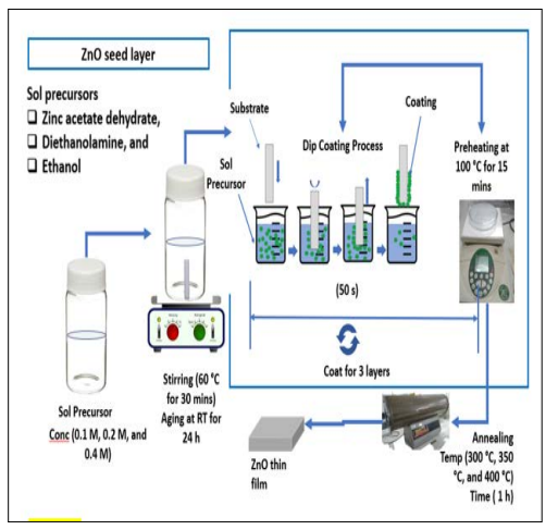
Figure 1: The ZnO Thin Film Preparation Process
The optical absorption spectra were measured using a UV-Vis (Shimadzu, model no. UV 3600) spectrophotometer with a wavelength range of 300-800 nm. The structural properties of the films were measured by using an X?ray diffractometer (XRD) (PW 3040/60 MPD X’pert pro-Panalytical Philips) with Cukα radiations (= 1.5406 Å) in the 2 range from 20° to 80°. High- resolution field emission scanning electron microscopy (FE-SEM, Model: NOVA NanoSEM 230) was used to examine the surface morphology of the nanoparticle’s thin films. The compositional property of thin films was observed using energy-dispersive X-ray spectra (EDX) spectroscopy attached to the FESEM unit.
Figures 2 (A) depict ZnO thin film absorbance spectra at varying sol concentration (0.1 M, 0.2 M, and 0.4 M). It was observed that all samples were absorbed with a slight shift towards a higher wavelength (red shift) below 400 nm in the ultraviolet region. This explained the electronic transition in ZnO from the valence band to the conduction band because of the quantum size of the particles [19]. Also, the uniform deposition of ZnO nanoparticles on the outer surface of the ITO glass substrate was confirmed. Figure 2 (B) displayed the bandgap energy for various sol concentration. The bandgap energy was estimated using Tauc’s relationship by extrapolating the straight-line portion of the plot of (αhv)2 versus (hv) using Equation 1.
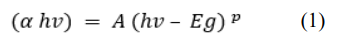
where α is the absorption coefficient, hv is the energy of incident photons, A is the function of the refractive index of the material, reduced mass, and speed of light, Eg is the energy band gap of the semiconductor, and the value of p equals due to ZnO being a direct bandgap material [21]. The calculated bandgap energy values (Eg) were 3.25 eV, 3.24 eV, and 3.18 eV, for 0.1 M, 0.2 M, and 0.4 M respectively. It is noticed that there was a decrease in bandgap energy with an increment in the sol precursor concentration. This decrease may be attributed to the crystallinity enhancement of the thin film produced, or the occurrence of defect states and disorder as concentration increased [22]. A similar trend was reported by Tan et al. on the effect of the sol concentration on the spin coating of ITO with ZnO nanoparticles [23]. As observed from Figure 3 (A), the bandgap energy values of the ZnO thin films were 3.22 eV, 3.18 eV and 3.18 eV for varying annealing temperature at 300 °C, 350 °C, and 400 °C respectively. A reduction in the values was observed as the temperature was raised from 300 °C to 400°C. This conforms with the trend reported by Al- Zahrani et al. for the effect of the annealing temperature on the performance of the ZnO seed layer for photoanode photoelectrochemical cells [24]. All the values obtained were in a close range to the standard value (3.37 eV) reported for bulk ZnO bandgap by previous studies [25].
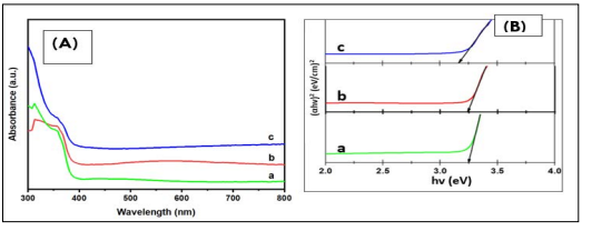
Figure 2: (A) UV-VIS Spectra (B) Bandgap Energy Curves of ZnO NPs at different sol Concentration:
Figure 3. (A): UV-VIS Spectra (B) Bandgap Energy Curves of ZnO NPs at different Annealing Temperatures: (a) 300 °C, (b) 350 °C and (c) 400 °C
The XRD diffractogram ZnO thin film under the influence of sol concentration and annealing temperature were presented in Figure 4 (a and b) respectively. The diffraction patterns demonstrate that the peaks of ZnO thin films produced are pure and have a good crystalline nature. The ZnO films produced exhibits wurtzite hexagonal structure (ICSD NO. 001-1317) with peaks identification of (010), (002), (011), (012), (110), (013), and (112) located at Bragg angles (2) of 31.77°, 34.43°, 36.27°, 47,55°, 56.61°, 63.01° and 68.11° respectively for concentration of sol precursor. For annealing temperature, peaks identification of (010), (002), (011), (012), (110), and (013) located at Bragg angles (2) of 31.72°, 34.43°, 36.26°, 47.50°, 56.61° and 63.01° respectively (ICSD No. 001-1317). Other peaks on the diffractograms reflect the contribution of the ITO substrates (ICSD No. 005-1986). Thus, the XRD patterns confirm the formation of ZnO thin films on the ITO glass substrate. Also, a highly preferred orientation was observed at the peak intensity (002), which increases with the corresponding increase in theconcentration of sol precursor. This shows the least surface energy and the ultimate atomic density that aids the film’s epitaxial growth was observed along the c-axis direction as the polar surface for the preferred orientation of crystallites [26, 27]. Similarly, other peaks which include (010) and (011) show a gradual development in intensity with the increase in the sol concentration [18]. The improvement at these peaks can be associated with the increase in density of the grain boundaries of thin films and variation in the initial concentration of the zinc for the growth of crystals and nucleation during the synthesis process [22, 26].
The average crystallite size was calculated by using Debye- Scherrer’s formula in Equation 2 [28].
where K is the Scherrer constant and the crystallite shape factor, represents the wavelength of the X-ray source used in XRD (1.5405), is full width at half maximum of diffraction peak, and is the Bragg angle of diffraction peak.
As inferred from Table 1 which shows the calculated average crystallite size and FWHM, the increase in the sol concentration and the annealing temperature decreased the full width at half maximum (FWHM) of (002) peak diffraction as depicted in Figure 4 This means that the crystallinity of the thin film becomes better by both molar concentration and annealing temperature. The size of the crystallite increased from 13.95 nm to 16.44 nm due to the increase in molar concentration [23]. The increase in the annealing temperature increased the crystallite from 11.12 nm to 17.95 nm. This indicates that the size of the grain is transformed from small to large with the increase in temperature [24]. Prior studies by reported that the crystalized size of ZnO thin films increased from 14.2 nm to 20.3 nm with an increase in temperature from 350 °C to 600 °C [29]. The plot of FWHM and crystallite size as a function of varying sol concentration and annealing temperature is demonstrated in Figure 5 and Figure 6.
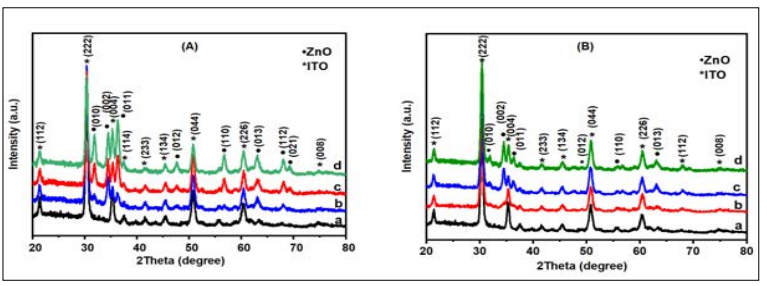
Figure 4: (A) X-ray Diffraction Patterns of ZnO Thin Films at different sol Concentration of (a) Plain ITO Glass, (b) 0,1 M, (c) 0.2 M and (d) 0.4 M and (B) Varying Annealing Temperature of (a) Plain ITO Glass, (b) 300 °C, (c) 350 °C and (d) 400 °C
|
Parameters |
Sample |
FWHM |
Crystallite size (002 peak), nm |
|
Concentration |
0.1 M |
0.5957 |
13.95 |
|
0.2 M |
0.5663 |
14.68 |
|
|
0.4 M |
0.5058 |
16.44 |
|
|
Temperature |
300 °C |
0.7473 |
11.12 |
|
350 °C |
0.5058 |
13.95 |
|
|
400 °C |
0.4632 |
17.95 |
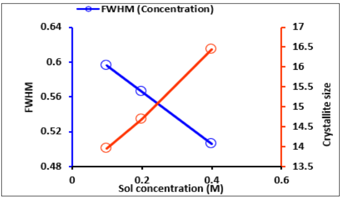
Figure 5: Plot of Crystallite Size and FWHM at Different Sol Concentrations
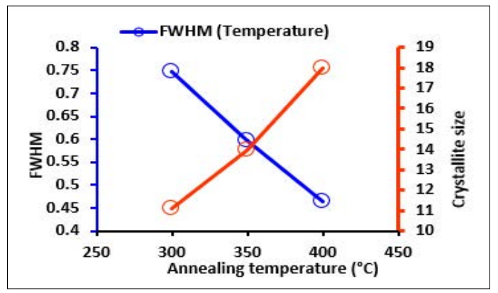
Figure 6: Plot of Crystallite Size and FWHM at Varying Annealing Temperature
The surface morphology of the thin films fabricated under different preparative conditions (sol concentration) is shown in Figures 6 (a, b and c). The ZnO thin films’ surface was uniformly distributed, homogenous, and well-compacted covering the ITO glass substrate completely.
With an increase in the sol concentration from 0.1 M to 0.2 M, an attraction between the main particles occurred by Van der Waals forces, forming bigger complexes which led to an increase of the average particle size from 12.86 nm to 26.45 nm. At a higher sol concentration (0.4 M), a larger number of grain boundaries and the surface of the film became a little rougher (Figure 7C) because of aggregation of secondary particles. This is in agreement with the report by Kamruzzaman & Zapien [30]. As observed in Figure 8 (a, b, and c), the thermal energy in the system was not sufficient to induce significant surface boundary fusion at 300 °C which resulted in the small grain size of the films produced because the ZnO molecules adsorption was not efficiently supported [24]. Based on the morphological and distribution changes, the thin films fabricated at 400 °C exhibit rougher surfaces compared to other thin films. This could be attributed to the increase in grain size at that temperature as evidenced from the XRD results. Therefore, adjusting the annealing temperature was key in determining the nanostructure orientation of ZnO nanoparticles. Furthermore, the results also demonstrated that the grain size, adhesion, and distribution of the ZnO nanoparticles are influenced by the annealing temperature.
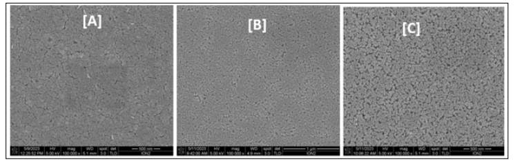
Figure 7: FESEM Images of ZnO NPs Prepared at Varying Concentration of Sol Precursor: (A) 0.1 M, (B) 0.2 M and (C) 0.4 M
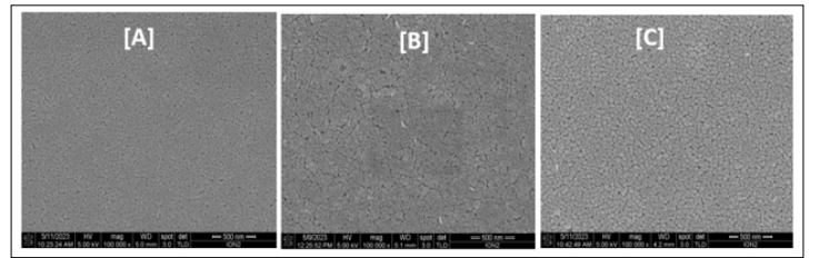
Figure 8: FESEM Images of ZnO NPs Prepared at Varying
Annealing Temperature of: (A) 300 °C, (B) 350 °C and (C) 400 °C
The EDX spectra of the sample at various preparative optimized conditions of sol concentration and annealing temperature are shown in Figure 9 (A, B and C) and Figure 10 (A, B and C). This confirms the ZnO thin film formation on the substrate. The spectrum peaks in the figures show the confirmation of Zn and O, while other peaks (Si and In) were from the ITO glass substrate used. The weight percentage and atomic percentage of each of the elements in the thin films are displayed as an inset on the Figures. It can be inferred from Figure 9 (A, B, and C) that the atomic percentage of Zn increases from 7.07 % - 27.92 % with an increase in sol concentration (0.1M – 0.4 M) while that of Si and In was observed to decrease as sol concentration increased suggesting improvement in the ZnO thin film thickness at higher molar concentration as evidenced in FESEM images. On the other hand, the atomic percentage of Zn was noticed to decrease from 7.98% to 6.39% with a rise in annealing temperature from 300 °C to 400 °C. The ITO glass constitutes an oxygen-rich environment as observed which resulted in the high atomic percentage of oxygen in all the prepared thin films as depicted in the inset on the figures [23].
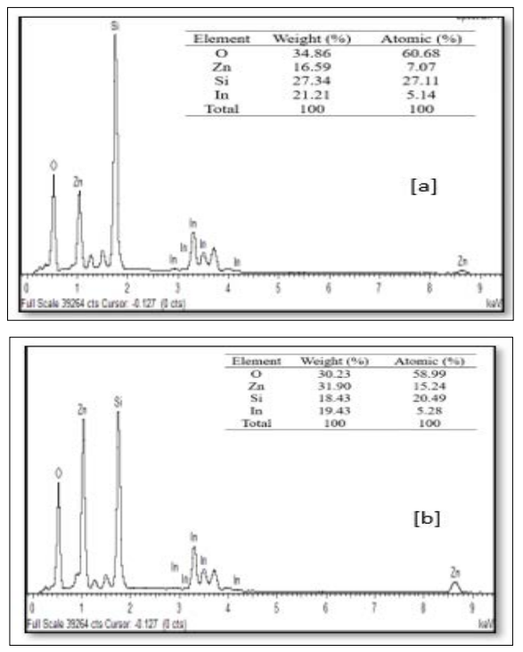
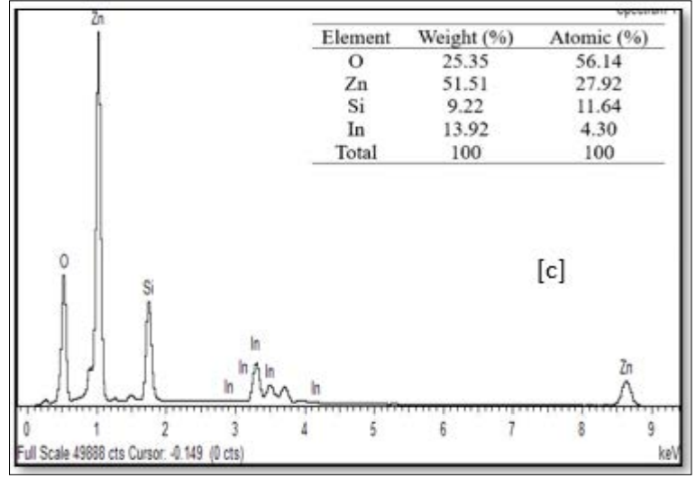
Figure 9: FESEM Images of ZnO Thin Films Prepared at Different Sol Precursor Concentration (a) 0.1 M, (b) 0.2 M and (c) 0.4 M
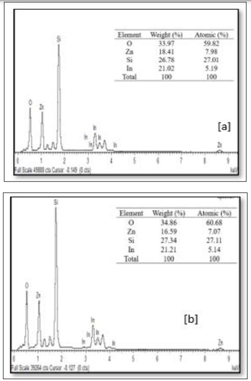
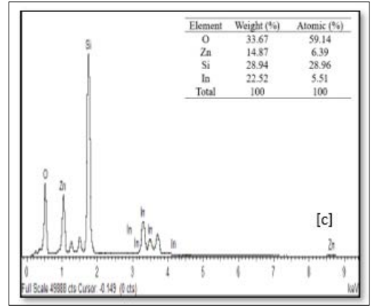
Figure 10: FESEM Images of ZnO Thin Films Prepared at Different Annealing Temperature of: (a) 300 °C, (b) 350 °C and (c) 400 °
Simple, affordable, eco-friendly, and convenient sol-gel dip coating methods have been successfully utilized for depositing ZnO thin film nanoparticles on ITO glass substrates. The results confirmed that the structural and morphological properties of ZnO thin films are strongly dependent on some preparative parameters including concentration of precursor and annealing temperature. No pronounced changes were noticed in the optical behavior of the ZnO thin films. All ZnO nanoparticle films exhibited a preferred (002) growth orientation with enhancement in the film quality, film crystallinity as well as grain size due to the increment in concentration of precursor and rise in annealing temperature.
The authors gratefully acknowledge the financial support provided by the Putra grant (GP-GPB/2021/9707600) for this work. They also extend their sincere appreciation to the Physics Department (Faculty of Science) and the Institute of Nanoscience and Nanotechnology at University Putra Malaysia for their invaluable assistance in conducting structural, optical, morphological, and compositional measurements. Special thanks are due to the Tertiary Education Trust Fund, Nigeria, for their financial support of Oloruntoba Sola Omodele’s PhD studies.