Author(s): Apoorva Reddy Proddutoori
The scaling of CMOS technology faces challenges as the demand rises, but FinFETs emerging as a vital alternative for 22nm technology node and lower. Otherwise, FinFETs tend to have multiple PVT variations, making static timing analysis (STA) more flexible and suitable to analyze the timing delay of the logic generation. Device simulation and statistical temporal analysis are used to derive PVT variation models for FinFET-based standard cell designs. Mixing different FinFET design styles shows promise in optimizing delays and leakage, as FinFETs offer better control of short-channel effects and processing scalability. Furthermore, lowering clock skew is also a prime design aspect to consider. However, as technology scales to smaller devices, process, voltage, and temperature (PVT) variations make minimizing clock distortion very difficult. To mitigate the effects of PVT variations, many previous works proposed a Post Silicon Tuning (PST) architecture to dynamically balance the skew of the clock tree. In this paper, we will disclose the details of clock tree synthesis optimizations and FinFET logic developments minimizing PVT variations.
In the previous decade of evolving technology ,static time analysis (STA) has been widely investigated to solve the problem of process variations, because static time analysis (STA) focuses on corner cases proved to be insufficient. In addition, microform technology computer-aided designsimulations have been used to study FinFETs behavior, but the computational complexity prevents TCAD from simulating large circuits with device simulations. Therefore, an efficient and accurate STA algorithm adapted for FinFET circuits must be developed. Finally, since the effects of supply voltage and temperature variations on the power and reference of FinFET circuits are significant, they should be considered together with process variations, in return affecting the over power and energy consumption.
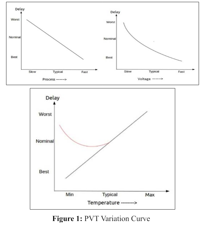
In CMOS technology, the transistor can be operated with drain to source voltages below 50 mV while in saturation. Reducing the gate-source voltage shifts the operation into the near or subthreshold regions. In these regions, the CMOS transistor operates with moderate or weak inversion at low drain current density, which limits the operating frequency of the logic design. To improve the inversion level, some strategies should be implemented, such as thick voltage, low or zero-threshold transistors and high Width to Length (W/L) transistor aspect ratio. These circuit logics are more complex than conventional circuits and complicate the task of analog design. In addition, circuits are very sensitive to process, voltage and temperature (PVT) variations, which increases the required design workload.
Moreover, microprocessors have streamlined the impact of high-performance processor architectures. In order to meet this rising demand to improve the capacity and density of the CMOS technology, a large portion of the die area is needed to be sacrificed. However, as we dive deeper into the sub-micron tech node, the shrinking size of each of the features has tremendously increased the stress on fabricating CMOS. Also, in CMOS fabrication leakage must be important parameter of consideration along with short-channel effect to eliminate process variations. Hence, FinFETs have become promising replacements for CMOS at the 22 nm node and beyond due to their better scalability, which provides the ability to maintain Moore's Law. FinFET is a non-planar dual gate device that provides tighter control of SCE, lower threshold leakage, and better scalability. In addition, independent control of two transistor gates in FinFETs enables some creative circuits and dynamic power/temperature management systems.
To perform the analysis of effect of PVT variations, this considers a subset of circuits representing the 1-4 input combinational cells most commonly available in traditional commercial standard cell libraries for CMOS at nano scale technology node. In this work, four main sources of variation in FinFET devices are investigated: gate length (l), fin height (h), fin width (w), and gate variation of work function. Diving depper into Analysis of the geometric and electrical variations of these parameters were made in for NFET and PFET devices. The study portrays that gate length and fin width have a significant deviating effect on ION and IOFF, respectively. However, the largest deviation effect in both currents is at the gate variation of work function, which causes a significant deviation in the total power, which must be considered in gate logic design. Further, highlighting the effect of process variability on the time and power of standard cells. This highlights the importance of considering gate variation of work function current and threshold voltage at an early stage of design, mainly in netlist generation tools for automatic layout generation.
Process variation is considered an important factor while scaling technology, because integrated circuits became more sensitive to parametric variations, and even small differences in the manufacturing process can be enough to change the behavior of the circuit design in total.
The comparison between 1-finFET devices and 16nm CMOS devices reveals that the former has higher power consumption. Single branch of PFET devices have specific current values, with PFET values slightly lower than NFET values. Further, while manufacturing the die the center area has different process variations when compared with respect to the boundary of the same die. FinFET technology devices shows a worst-case scenario with 2.7 times higher transient current values compared to CMOS devices. CMOS Bulk technology has lower average power deviation compared to FinFET technology, which experiences up to >150% deviation from expected values.
The sensitivity to process variations is less than 9% for all standard cell libraries variations in terms of power deviation. In terms of delay results, FinFET standard library cells offer a higher speedup compared to bulk CMOS versions, but are more sensitive to process variation, especially in terms of gate variations of work function. Additionally, the following factors impact process variations of the die; UV light wavelength, gate oxide thickness variations, transistor width, mobility fluctuations, doping concentration and many more.
The supply voltage can vary along the circuit, for example due to an imbalance in the power distribution network. Therefore, a part of this paper evaluates the effect of supply voltage fluctuations on the cell. For AND, NOR, OR, and FA cells, the frequency of activity was reduced to allow near-threshold activity in voltage experiments. Therefore, these circuits do not consume power at low temperature and voltage values. This is because these cells spend more time in static activity. The higher voltage than the temperature tests.
Like the process variations parameters, the supply voltage Vdd can also vary depending on the logic design. The presence of IR degradation and unbalanced power distribution networks put more pressure on circuit designers to meet durability and power limitations during supply voltage Vdd switching. The voltage Vdd can also exceed its nominal value based on the designs of the voltage divider in the circuit. Therefore, we consider the change of Vdd in positive and negative directions. In addition to directly affecting leakage power and dynamic or switching power, Vdd also affects the timing behavior of logic gates by determining the gate drive. This is because the power is transmitted through the circuit through a power distribution network.
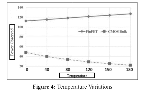
All CMOS versions of the same technology show similar behavior in delay, total power, static current and temperature changes. For the sake of brevity, only the average values for each skill are assessed. Figure 3 and 4 show how temperature affects performance of CMOS behavior are generally different and different layouts of FinFET. Advanced CMOS technology delay increases with temperature, in contrary, FinFET standard library cells portray a slight delay decrease of 8% for a single degree temperature change. Total power consumption represents a different situation. FinFET technology has a smaller impact, but the total power consumption is higher, but the differences are small.
However, the temperature drop has a positive effect on the overall power consumption and energy dissipation of CMOS technology.
The power consumption drops significantly as the temperature rises, exhibiting high sensitivity under adverse conditions.
A practical implementation of delay buffer includes a 3-bit control signal which results in eight different delays. For ease of application most delay buffers have the same delay for each delay step. The design problem with using delay buffers is the discreteness of its adjustable delay. In a structure the delay can be adjusted to only eight possible different values. The space between two consecutive delays is called delay buffer resolution. Besides the solution, the problem is also the harmonization of the solution. Ideally, we do each solution with the same delay. In practical models, however, it is very difficult to make the value of the delay linear, the relationship between the control value and the delay, as well as the difference in delay between two consecutive values of the operation.
The main purpose of the PST architecture is to tolerate PVT variations, PVT variations may still affect the accuracy or functionality of the PST architecture. As a result, PVT variations can also affect the tolerance of the PST architecture. Thus, robustness testing of the PST architecture becomes a very important task. However, the traditional method of logic gate testing is not suitable for testing ADBs and PDs. The reasons are as follows. First, unlike faulty logic gates, which can cause operational errors, errors in the PST architecture only affect clock skew. As a result, we are not able to detect the failure of the PST architecture directly from the project output. Second, traditional test methodology tests a chip under specific environmental conditions, while testing a PST architecture requires it to be done under many different environmental conditions. It is also not easy to create PVT variants in the test environment. As a result, even if a manufactured chip passes routine tests, we cannot guarantee that the PST architecture can dynamically minimize clock distortion under various environmental conditions. Finally, failure modeling is also a big problem for testing PST architectures because there are many different devices such as ADBs and PDs. It is very difficult to find a good failure model for the PST architecture [1-11].